Page 3 of 3
Re: Assembling Gigatron the hard way
Posted: 30 Apr 2019, 08:26
by marcelk
It's probably fastest to do a continuity test on all breadboard connections using the schematic as a reference. It may take 1 or 2 hours, but then you know everything is wired correctly.
Don't worry too much about the difference between CLK2 and CLK1. With the parts that are provided with the kit, you can even keep them the same. In fact, if the shift is too much, nothing will work.
Re: Assembling Gigatron the hard way
Posted: 30 Apr 2019, 10:35
by pythag
I've finally made it past the instruction at 0x0A!!!
In the end I tracked it down using logic.... the bus having 1100 0000 and the AC register having 1100 1111 during the XOR suggested something was mixed up with the bus connections to the ALU. To confirm it was within the ALU I disconnected the ALU outputs one at a time and sourced them from 0 then 1 and confirmed the correct bits in the AC register were updated during the XOR (they were). It actually turned out that the order of 4 high bit inputs to the 4-bit adders was swapped.
I probably could have seen that coming - attached is a photo of the sheet my son was working from when he wired ALU and the reason for the mistake is fairly obvious... (he clearly doesn't know his alphabet!!!)
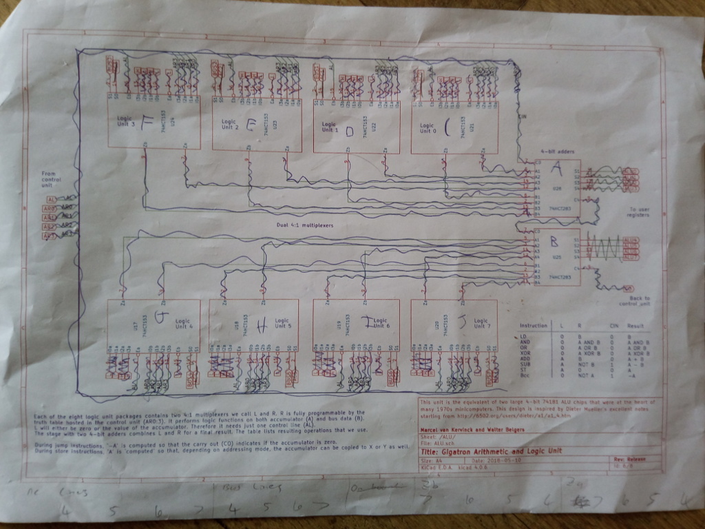
- IMG_20190501_091226.jpg (254.24 KiB) Viewed 8341 times
So.... straw poll... Do I now either:
a) Take it off life support (remove the Arduino), let the clock run free and see what happens?
...or...
b) Modify my Arduino tester to run the clock at progressively higher rates (I'll never reach 6.25Mhz though) and see it all still looks good?
Just on the off chance it's of any use to anyone else later, here is a dump of my signals during the memory test loop:
Code: Select all
Reset
Clock cycle:0
ROM ADR:0000 BUS:00 (000000000) Data:80 (010000000)
IR:00 [ins:0-LD  00011 mod:0-1110 bus-0000-ROM W:0 J:0 LD:0 ]
Y:00 (000000000) AC:00 (000000000) YL:1 XL:1 EH:1 EL:1 OL:1 LD:0 PL:1 PH:1

Clock cycle:1  ROM Lookup: IR:0 D:0

ROM ADR:0001 BUS:00 (000000000) Data:80 (010000000)
IR:00 [ins:0-LD  00011 mod:0-1110 bus-0000-ROM W:0 J:0 LD:0 ]
Y:00 (000000000) AC:00 (000000000) YL:1 XL:1 EH:1 EL:1 OL:1 LD:0 PL:1 PH:1

PC:1 IR:00 [ins:0-LD  00011 mod:0-1110 bus-0000-ROM W:0 J:0 LD:0 ]
D:00 AC:00 (000000000) X:00 Y:00
YL:1 XL:1 EH:1 EL:1 OL:1 LD:0 PL:1 PH:1 CO:0 AC7:0
---------------
Clock cycle:2  ROM Lookup: IR:18 D:80

ROM ADR:0002 BUS:80 (010000000) Data:B0 (010110000)
IR:18 [ins:0-LD  00011 mod:6-1101 bus-0000-ROM W:0 J:0 LD:1 ]
Y:00 (000000000) AC:00 (000000000) YL:1 XL:1 EH:1 EL:1 OL:0 LD:1 PL:1 PH:1

PC:2 IR:18 [ins:0-LD  00011 mod:6-1101 bus-0000-ROM W:0 J:0 LD:1 ]
D:80 AC:00 (000000000) X:00 Y:00
YL:1 XL:1 EH:1 EL:1 OL:0 LD:1 PL:1 PH:1 CO:0 AC7:0
---------------
Clock cycle:3  ROM Lookup: IR:18 D:C0

ROM ADR:0003 BUS:C0 (011000000) Data:A0 (010100000)
IR:18 [ins:0-LD  00011 mod:6-1101 bus-0000-ROM W:0 J:0 LD:1 ]
Y:00 (000000000) AC:00 (000000000) YL:1 XL:1 EH:1 EL:1 OL:0 LD:1 PL:1 PH:1

PC:3 IR:18 [ins:0-LD  00011 mod:6-1101 bus-0000-ROM W:0 J:0 LD:1 ]
D:C0 AC:00 (000000000) X:00 Y:00
YL:1 XL:1 EH:1 EL:1 OL:0 LD:1 PL:1 PH:1 CO:0 AC7:0
---------------
Clock cycle:4  ROM Lookup: IR:0 D:1

ROM ADR:0004 BUS:01 (000000001) Data:80 (010000000)
IR:00 [ins:0-LD  00011 mod:0-1110 bus-0000-ROM W:0 J:0 LD:0 ]
Y:00 (000000000) AC:01 (000000001) YL:1 XL:1 EH:1 EL:1 OL:1 LD:0 PL:1 PH:1

PC:4 IR:00 [ins:0-LD  00011 mod:0-1110 bus-0000-ROM W:0 J:0 LD:0 ]
D:01 AC:00 (000000000) X:00 Y:00
YL:1 XL:1 EH:1 EL:1 OL:1 LD:0 PL:1 PH:1 CO:0 AC7:0
---------------
Clock cycle:5  ROM Lookup: IR:D6 D:1

ROM ADR:0005 BUS:01 (000000001) Data:22 (000100010)
IR:D6 [ins:6-ST  11111 mod:5-1111 bus-0010-AC  W:1 J:0 LD:1 ]
Y:00 (000000000) AC:01 (000000001) YL:0 XL:0 EH:1 EL:1 OL:1 LD:1 PL:1 PH:1

PC:5 IR:D6 [ins:6-ST  11111 mod:5-1111 bus-0010-AC  W:1 J:0 LD:1 ]
D:01 AC:01 (000000001) X:00 Y:00
YL:0 XL:0 EH:1 EL:1 OL:1 LD:1 PL:1 PH:1 CO:0 AC7:0
---------------
Clock cycle:6  ROM Lookup: IR:0 D:FF

ROM ADR:0006 BUS:FF (011111111) Data:88 (010001000)
IR:00 [ins:0-LD  00011 mod:0-1110 bus-0000-ROM W:0 J:0 LD:0 ]
Y:00 (000000000) AC:FF (011111111) YL:1 XL:1 EH:1 EL:1 OL:1 LD:0 PL:1 PH:1

Writing 1 to address 1
PC:6 IR:00 [ins:0-LD  00011 mod:0-1110 bus-0000-ROM W:0 J:0 LD:0 ]
D:FF AC:01 (000000001) X:00 Y:01
YL:1 XL:1 EH:1 EL:1 OL:1 LD:0 PL:1 PH:1 CO:0 AC7:0
---------------
Clock cycle:7  ROM Lookup: IR:69 D:0

ROM ADR:0007 BUS:CF (011001111) Data:B8 (010111000)
IR:69 [ins:3-XOR 01001 mod:2-0110 bus-0001-RAM W:0 J:0 LD:0 ]
Y:00 (000000000) AC:30 (000110000) YL:1 XL:1 EH:0 EL:1 OL:1 LD:0 PL:1 PH:1

PC:7 IR:69 [ins:3-XOR 01001 mod:2-0110 bus-0001-RAM W:0 J:0 LD:0 ]
D:00 AC:FF (011111111) X:00 Y:01
YL:1 XL:1 EH:0 EL:1 OL:1 LD:0 PL:1 PH:1 CO:0 AC7:1
---------------
Clock cycle:8  ROM Lookup: IR:CA D:0

ROM ADR:0008 BUS:30 (000110000) Data:28 (000101000)
IR:CA [ins:6-ST  11111 mod:2-0110 bus-0010-AC  W:1 J:0 LD:1 ]
Y:00 (000000000) AC:30 (000110000) YL:1 XL:1 EH:0 EL:1 OL:1 LD:1 PL:1 PH:1

Read uninit from 256
PC:8 IR:CA [ins:6-ST  11111 mod:2-0110 bus-0010-AC  W:1 J:0 LD:1 ]
D:00 AC:00 (000000000) X:00 Y:01
YL:1 XL:1 EH:0 EL:1 OL:1 LD:1 PL:1 PH:1 CO:0 AC7:0
---------------
Clock cycle:9  ROM Lookup: IR:C2 D:0

ROM ADR:0009 BUS:30 (000110000) Data:08 (000001000)
IR:C2 [ins:6-ST  11111 mod:0-1110 bus-0010-AC  W:1 J:0 LD:1 ]
Y:00 (000000000) AC:30 (000110000) YL:1 XL:1 EH:1 EL:1 OL:1 LD:1 PL:1 PH:1

Writing 0 to address 256
PC:9 IR:C2 [ins:6-ST  11111 mod:0-1110 bus-0010-AC  W:1 J:0 LD:1 ]
D:00 AC:00 (000000000) X:00 Y:01
YL:1 XL:1 EH:1 EL:1 OL:1 LD:1 PL:1 PH:1 CO:0 AC7:0
---------------
Clock cycle:10  ROM Lookup: IR:69 D:0

ROM ADR:000A BUS:30 (000110000) Data:E0 (011100000)
IR:69 [ins:3-XOR 01001 mod:2-0110 bus-0001-RAM W:0 J:0 LD:0 ]
Y:00 (000000000) AC:00 (000000000) YL:1 XL:1 EH:0 EL:1 OL:1 LD:0 PL:1 PH:1

Writing 0 to address 0
PC:10 IR:69 [ins:3-XOR 01001 mod:2-0110 bus-0001-RAM W:0 J:0 LD:0 ]
D:00 AC:00 (000000000) X:00 Y:01
YL:1 XL:1 EH:0 EL:1 OL:1 LD:0 PL:1 PH:1 CO:0 AC7:0
---------------
Clock cycle:11  ROM Lookup: IR:EC D:A

ROM ADR:000B BUS:0A (000001010) Data:A6 (010100110)
IR:EC [ins:7-BCC 01010 mod:3-1111 bus-0000-ROM W:0 J:1-cond LD:1 ]
Y:00 (000000000) AC:00 (000000000) YL:1 XL:1 EH:1 EL:1 OL:1 LD:1 PL:1 PH:1

Read 0 from 256
PC:11 IR:EC [ins:7-BCC 01010 mod:3-1111 bus-0000-ROM W:0 J:1-cond LD:1 ]
D:0A AC:00 (000000000) X:00 Y:01
YL:1 XL:1 EH:1 EL:1 OL:1 LD:1 PL:0 PH:1 CO:0 AC7:0
---------------
=== Yay! We finally made it here!!!! ===

Clock cycle:12  ROM Lookup: IR:0 D:FF

ROM ADR:000C BUS:FF (011111111) Data:88 (010001000)
IR:00 [ins:0-LD  00011 mod:0-1110 bus-0000-ROM W:0 J:0 LD:0 ]
Y:80 (010000000) AC:FF (011111111) YL:1 XL:1 EH:1 EL:1 OL:1 LD:0 PL:1 PH:1

PC:12 IR:00 [ins:0-LD  00011 mod:0-1110 bus-0000-ROM W:0 J:0 LD:0 ]
D:FF AC:00 (000000000) X:00 Y:01
YL:1 XL:1 EH:1 EL:1 OL:1 LD:0 PL:1 PH:1 CO:0 AC7:0
---------------
Clock cycle:13  ROM Lookup: IR:69 D:0

ROM ADR:000D BUS:30 (000110000) Data:A0 (010100000)
IR:69 [ins:3-XOR 01001 mod:2-0110 bus-0001-RAM W:0 J:0 LD:0 ]
Y:00 (000000000) AC:CF (011001111) YL:1 XL:1 EH:0 EL:1 OL:1 LD:0 PL:1 PH:1

PC:13 IR:69 [ins:3-XOR 01001 mod:2-0110 bus-0001-RAM W:0 J:0 LD:0 ]
D:00 AC:FF (011111111) X:00 Y:01
YL:1 XL:1 EH:0 EL:1 OL:1 LD:0 PL:1 PH:1 CO:0 AC7:1
---------------
Clock cycle:14  ROM Lookup: IR:CA D:0

ROM ADR:000E BUS:CF (011001111) Data:20 (000100000)
IR:CA [ins:6-ST  11111 mod:2-0110 bus-0010-AC  W:1 J:0 LD:1 ]
Y:00 (000000000) AC:CF (011001111) YL:1 XL:1 EH:0 EL:1 OL:1 LD:1 PL:1 PH:1

Read 0 from 256
PC:14 IR:CA [ins:6-ST  11111 mod:2-0110 bus-0010-AC  W:1 J:0 LD:1 ]
D:00 AC:FF (011111111) X:00 Y:01
YL:1 XL:1 EH:0 EL:1 OL:1 LD:1 PL:1 PH:1 CO:0 AC7:1
---------------
Clock cycle:15  ROM Lookup: IR:61 D:0

ROM ADR:000F BUS:30 (000110000) Data:80 (010000000)
IR:61 [ins:3-XOR 01001 mod:0-1110 bus-0001-RAM W:0 J:0 LD:0 ]
Y:00 (000000000) AC:20 (000100000) YL:1 XL:1 EH:1 EL:1 OL:1 LD:0 PL:1 PH:1

Writing 255 to address 256
PC:15 IR:61 [ins:3-XOR 01001 mod:0-1110 bus-0001-RAM W:0 J:0 LD:0 ]
D:00 AC:FF (011111111) X:00 Y:01
YL:1 XL:1 EH:1 EL:1 OL:1 LD:0 PL:1 PH:1 CO:0 AC7:1
---------------
Clock cycle:16  ROM Lookup: IR:F0 D:13

ROM ADR:0010 BUS:13 (000010011) Data:A0 (010100000)
IR:F0 [ins:7-BCC 01010 mod:4-1111 bus-0000-ROM W:0 J:1-cond LD:1 ]
Y:00 (000000000) AC:20 (000100000) YL:1 XL:1 EH:1 EL:1 OL:1 LD:1 PL:1 PH:1

Read 0 from 0
PC:16 IR:F0 [ins:7-BCC 01010 mod:4-1111 bus-0000-ROM W:0 J:1-cond LD:1 ]
D:13 AC:FF (011111111) X:00 Y:01
YL:1 XL:1 EH:1 EL:1 OL:1 LD:1 PL:1 PH:1 CO:0 AC7:1
---------------
Clock cycle:17  ROM Lookup: IR:1 D:1

ROM ADR:0011 BUS:01 (000000001) Data:80 (010000000)
IR:01 [ins:0-LD  00011 mod:0-1110 bus-0001-RAM W:0 J:0 LD:0 ]
Y:00 (000000000) AC:01 (000000001) YL:1 XL:1 EH:1 EL:1 OL:1 LD:0 PL:1 PH:1

PC:17 IR:01 [ins:0-LD  00011 mod:0-1110 bus-0001-RAM W:0 J:0 LD:0 ]
D:01 AC:FF (011111111) X:00 Y:01
YL:1 XL:1 EH:1 EL:1 OL:1 LD:0 PL:1 PH:1 CO:0 AC7:1
---------------
Clock cycle:18  ROM Lookup: IR:FC D:4

ROM ADR:0012 BUS:04 (000000100) Data:A3 (010100011)
IR:FC [ins:7-BCC 01010 mod:7-1111 bus-0000-ROM W:0 J:1-cond LD:1 ]
Y:00 (000000000) AC:01 (000000001) YL:1 XL:1 EH:1 EL:1 OL:1 LD:1 PL:0 PH:1

Read 1 from 1
PC:18 IR:FC [ins:7-BCC 01010 mod:7-1111 bus-0000-ROM W:0 J:1-cond LD:1 ]
D:04 AC:01 (000000001) X:00 Y:01
YL:1 XL:1 EH:1 EL:1 OL:1 LD:1 PL:0 PH:1 CO:0 AC7:0
---------------
Clock cycle:19  ROM Lookup: IR:0 D:1

ROM ADR:0004 BUS:02 (000000010) Data:00 (000000000)
IR:82 [ins:4-ADD 10011 mod:0-1110 bus-0010-AC  W:0 J:0 LD:0 ]
Y:00 (000000000) AC:02 (000000010) YL:1 XL:1 EH:1 EL:1 OL:1 LD:0 PL:1 PH:1

PC:4 IR:82 [ins:4-ADD 10011 mod:0-1110 bus-0010-AC  W:0 J:0 LD:0 ]
D:00 AC:01 (000000001) X:00 Y:01
YL:1 XL:1 EH:1 EL:1 OL:1 LD:0 PL:1 PH:1 CO:0 AC7:0
---------------
Clock cycle:20  ROM Lookup: IR:D6 D:1

ROM ADR:0005 BUS:02 (000000010) Data:22 (000100010)
IR:D6 [ins:6-ST  11111 mod:5-1111 bus-0010-AC  W:1 J:0 LD:1 ]
Y:00 (000000000) AC:02 (000000010) YL:0 XL:0 EH:1 EL:1 OL:1 LD:1 PL:1 PH:1

PC:5 IR:D6 [ins:6-ST  11111 mod:5-1111 bus-0010-AC  W:1 J:0 LD:1 ]
D:01 AC:02 (000000010) X:00 Y:01
YL:0 XL:0 EH:1 EL:1 OL:1 LD:1 PL:1 PH:1 CO:0 AC7:0
---------------
Clock cycle:21  ROM Lookup: IR:0 D:FF

ROM ADR:0006 BUS:FF (011111111) Data:88 (010001000)
IR:00 [ins:0-LD  00011 mod:0-1110 bus-0000-ROM W:0 J:0 LD:0 ]
Y:80 (010000000) AC:FF (011111111) YL:1 XL:1 EH:1 EL:1 OL:1 LD:0 PL:1 PH:1

Writing 2 to address 1
PC:6 IR:00 [ins:0-LD  00011 mod:0-1110 bus-0000-ROM W:0 J:0 LD:0 ]
D:FF AC:02 (000000010) X:00 Y:02
YL:1 XL:1 EH:1 EL:1 OL:1 LD:0 PL:1 PH:1 CO:0 AC7:0
---------------
Clock cycle:22  ROM Lookup: IR:69 D:0

ROM ADR:0007 BUS:7E (001111110) Data:A0 (010100000)
IR:69 [ins:3-XOR 01001 mod:2-0110 bus-0001-RAM W:0 J:0 LD:0 ]
Y:00 (000000000) AC:81 (010000001) YL:1 XL:1 EH:0 EL:1 OL:1 LD:0 PL:1 PH:1

PC:7 IR:69 [ins:3-XOR 01001 mod:2-0110 bus-0001-RAM W:0 J:0 LD:0 ]
D:00 AC:FF (011111111) X:00 Y:02
YL:1 XL:1 EH:0 EL:1 OL:1 LD:0 PL:1 PH:1 CO:0 AC7:1
---------------
Clock cycle:23  ROM Lookup: IR:CA D:0

ROM ADR:0008 BUS:81 (010000001) Data:20 (000100000)
IR:CA [ins:6-ST  11111 mod:2-0110 bus-0010-AC  W:1 J:0 LD:1 ]
Y:00 (000000000) AC:81 (010000001) YL:1 XL:1 EH:0 EL:1 OL:1 LD:1 PL:1 PH:1

Read uninit from 512
PC:8 IR:CA [ins:6-ST  11111 mod:2-0110 bus-0010-AC  W:1 J:0 LD:1 ]
D:00 AC:00 (000000000) X:00 Y:02
YL:1 XL:1 EH:0 EL:1 OL:1 LD:1 PL:1 PH:1 CO:0 AC7:0
---------------
Clock cycle:24  ROM Lookup: IR:C2 D:0

ROM ADR:0009 BUS:81 (010000001) Data:00 (000000000)
IR:C2 [ins:6-ST  11111 mod:0-1110 bus-0010-AC  W:1 J:0 LD:1 ]
Y:00 (000000000) AC:81 (010000001) YL:1 XL:1 EH:1 EL:1 OL:1 LD:1 PL:1 PH:1

Writing 0 to address 512
PC:9 IR:C2 [ins:6-ST  11111 mod:0-1110 bus-0010-AC  W:1 J:0 LD:1 ]
D:00 AC:00 (000000000) X:00 Y:02
YL:1 XL:1 EH:1 EL:1 OL:1 LD:1 PL:1 PH:1 CO:0 AC7:0
---------------
Clock cycle:25  ROM Lookup: IR:69 D:0

ROM ADR:000A BUS:81 (010000001) Data:E0 (011100000)
IR:69 [ins:3-XOR 01001 mod:2-0110 bus-0001-RAM W:0 J:0 LD:0 ]
Y:00 (000000000) AC:00 (000000000) YL:1 XL:1 EH:0 EL:1 OL:1 LD:0 PL:1 PH:1

Writing 0 to address 0
PC:10 IR:69 [ins:3-XOR 01001 mod:2-0110 bus-0001-RAM W:0 J:0 LD:0 ]
D:00 AC:00 (000000000) X:00 Y:02
YL:1 XL:1 EH:0 EL:1 OL:1 LD:0 PL:1 PH:1 CO:0 AC7:0
---------------
Clock cycle:26  ROM Lookup: IR:EC D:A

ROM ADR:000B BUS:0A (000001010) Data:E6 (011100110)
IR:EC [ins:7-BCC 01010 mod:3-1111 bus-0000-ROM W:0 J:1-cond LD:1 ]
Y:00 (000000000) AC:00 (000000000) YL:1 XL:1 EH:1 EL:1 OL:1 LD:1 PL:1 PH:1

Read 0 from 512
PC:11 IR:EC [ins:7-BCC 01010 mod:3-1111 bus-0000-ROM W:0 J:1-cond LD:1 ]
D:0A AC:00 (000000000) X:00 Y:02
YL:1 XL:1 EH:1 EL:1 OL:1 LD:1 PL:0 PH:1 CO:0 AC7:0
---------------
Clock cycle:27  ROM Lookup: IR:0 D:FF

ROM ADR:000C BUS:FF (011111111) Data:88 (010001000)
IR:00 [ins:0-LD  00011 mod:0-1110 bus-0000-ROM W:0 J:0 LD:0 ]
Y:80 (010000000) AC:FF (011111111) YL:1 XL:1 EH:1 EL:1 OL:1 LD:0 PL:1 PH:1

PC:12 IR:00 [ins:0-LD  00011 mod:0-1110 bus-0000-ROM W:0 J:0 LD:0 ]
D:FF AC:00 (000000000) X:00 Y:02
YL:1 XL:1 EH:1 EL:1 OL:1 LD:0 PL:1 PH:1 CO:0 AC7:0
---------------
Clock cycle:28  ROM Lookup: IR:69 D:0

ROM ADR:000D BUS:81 (010000001) Data:A8 (010101000)
IR:69 [ins:3-XOR 01001 mod:2-0110 bus-0001-RAM W:0 J:0 LD:0 ]
Y:00 (000000000) AC:7E (001111110) YL:1 XL:1 EH:0 EL:1 OL:1 LD:0 PL:1 PH:1

PC:13 IR:69 [ins:3-XOR 01001 mod:2-0110 bus-0001-RAM W:0 J:0 LD:0 ]
D:00 AC:FF (011111111) X:00 Y:02
YL:1 XL:1 EH:0 EL:1 OL:1 LD:0 PL:1 PH:1 CO:0 AC7:1
---------------
Clock cycle:29  ROM Lookup: IR:CA D:0

ROM ADR:000E BUS:7E (001111110) Data:28 (000101000)
IR:CA [ins:6-ST  11111 mod:2-0110 bus-0010-AC  W:1 J:0 LD:1 ]
Y:00 (000000000) AC:7E (001111110) YL:1 XL:1 EH:0 EL:1 OL:1 LD:1 PL:1 PH:1

Read 0 from 512
PC:14 IR:CA [ins:6-ST  11111 mod:2-0110 bus-0010-AC  W:1 J:0 LD:1 ]
D:00 AC:FF (011111111) X:00 Y:02
YL:1 XL:1 EH:0 EL:1 OL:1 LD:1 PL:1 PH:1 CO:0 AC7:1
---------------
Clock cycle:30  ROM Lookup: IR:61 D:0

ROM ADR:000F BUS:81 (010000001) Data:88 (010001000)
IR:61 [ins:3-XOR 01001 mod:0-1110 bus-0001-RAM W:0 J:0 LD:0 ]
Y:00 (000000000) AC:FF (011111111) YL:1 XL:1 EH:1 EL:1 OL:1 LD:0 PL:1 PH:1

Writing 255 to address 512
PC:15 IR:61 [ins:3-XOR 01001 mod:0-1110 bus-0001-RAM W:0 J:0 LD:0 ]
D:00 AC:FF (011111111) X:00 Y:02
YL:1 XL:1 EH:1 EL:1 OL:1 LD:0 PL:1 PH:1 CO:0 AC7:1
---------------
Clock cycle:31  ROM Lookup: IR:F0 D:13

ROM ADR:0010 BUS:13 (000010011) Data:A8 (010101000)
IR:F0 [ins:7-BCC 01010 mod:4-1111 bus-0000-ROM W:0 J:1-cond LD:1 ]
Y:00 (000000000) AC:FF (011111111) YL:1 XL:1 EH:1 EL:1 OL:1 LD:1 PL:1 PH:1

Read 0 from 0
PC:16 IR:F0 [ins:7-BCC 01010 mod:4-1111 bus-0000-ROM W:0 J:1-cond LD:1 ]
D:13 AC:FF (011111111) X:00 Y:02
YL:1 XL:1 EH:1 EL:1 OL:1 LD:1 PL:1 PH:1 CO:0 AC7:1
---------------
Clock cycle:32  ROM Lookup: IR:1 D:1

ROM ADR:0011 BUS:02 (000000010) Data:80 (010000000)
IR:01 [ins:0-LD  00011 mod:0-1110 bus-0001-RAM W:0 J:0 LD:0 ]
Y:00 (000000000) AC:02 (000000010) YL:1 XL:1 EH:1 EL:1 OL:1 LD:0 PL:1 PH:1

PC:17 IR:01 [ins:0-LD  00011 mod:0-1110 bus-0001-RAM W:0 J:0 LD:0 ]
D:01 AC:FF (011111111) X:00 Y:02
YL:1 XL:1 EH:1 EL:1 OL:1 LD:0 PL:1 PH:1 CO:0 AC7:1
---------------
Clock cycle:33  ROM Lookup: IR:FC D:4

ROM ADR:0012 BUS:04 (000000100) Data:A3 (010100011)
IR:FC [ins:7-BCC 01010 mod:7-1111 bus-0000-ROM W:0 J:1-cond LD:1 ]
Y:00 (000000000) AC:02 (000000010) YL:1 XL:1 EH:1 EL:1 OL:1 LD:1 PL:0 PH:1

Read 2 from 1
PC:18 IR:FC [ins:7-BCC 01010 mod:7-1111 bus-0000-ROM W:0 J:1-cond LD:1 ]
D:04 AC:02 (000000010) X:00 Y:02
YL:1 XL:1 EH:1 EL:1 OL:1 LD:1 PL:0 PH:1 CO:0 AC7:0
---------------
Clock cycle:34  ROM Lookup: IR:0 D:1

ROM ADR:0004 BUS:04 (000000100) Data:00 (000000000)
IR:82 [ins:4-ADD 10011 mod:0-1110 bus-0010-AC  W:0 J:0 LD:0 ]
Y:00 (000000000) AC:04 (000000100) YL:1 XL:1 EH:1 EL:1 OL:1 LD:0 PL:1 PH:1

PC:4 IR:82 [ins:4-ADD 10011 mod:0-1110 bus-0010-AC  W:0 J:0 LD:0 ]
D:00 AC:02 (000000010) X:00 Y:02
YL:1 XL:1 EH:1 EL:1 OL:1 LD:0 PL:1 PH:1 CO:0 AC7:0
---------------
Clock cycle:35  ROM Lookup: IR:D6 D:1

ROM ADR:0005 BUS:04 (000000100) Data:22 (000100010)
IR:D6 [ins:6-ST  11111 mod:5-1111 bus-0010-AC  W:1 J:0 LD:1 ]
Y:00 (000000000) AC:04 (000000100) YL:0 XL:0 EH:1 EL:1 OL:1 LD:1 PL:1 PH:1

PC:5 IR:D6 [ins:6-ST  11111 mod:5-1111 bus-0010-AC  W:1 J:0 LD:1 ]
D:01 AC:04 (000000100) X:00 Y:02
YL:0 XL:0 EH:1 EL:1 OL:1 LD:1 PL:1 PH:1 CO:0 AC7:0
---------------
Clock cycle:36  ROM Lookup: IR:0 D:FF

ROM ADR:0006 BUS:FF (011111111) Data:88 (010001000)
IR:00 [ins:0-LD  00011 mod:0-1110 bus-0000-ROM W:0 J:0 LD:0 ]
Y:80 (010000000) AC:FF (011111111) YL:1 XL:1 EH:1 EL:1 OL:1 LD:0 PL:1 PH:1

Writing 4 to address 1
PC:6 IR:00 [ins:0-LD  00011 mod:0-1110 bus-0000-ROM W:0 J:0 LD:0 ]
D:FF AC:04 (000000100) X:00 Y:04
YL:1 XL:1 EH:1 EL:1 OL:1 LD:0 PL:1 PH:1 CO:0 AC7:0
---------------
Clock cycle:37  ROM Lookup: IR:69 D:0

ROM ADR:0007 BUS:F7 (011110111) Data:E0 (011100000)
IR:69 [ins:3-XOR 01001 mod:2-0110 bus-0001-RAM W:0 J:0 LD:0 ]
Y:00 (000000000) AC:08 (000001000) YL:1 XL:1 EH:0 EL:1 OL:1 LD:0 PL:1 PH:1

PC:7 IR:69 [ins:3-XOR 01001 mod:2-0110 bus-0001-RAM W:0 J:0 LD:0 ]
D:00 AC:FF (011111111) X:00 Y:04
YL:1 XL:1 EH:0 EL:1 OL:1 LD:0 PL:1 PH:1 CO:0 AC7:1
---------------
Clock cycle:38  ROM Lookup: IR:CA D:0

ROM ADR:0008 BUS:08 (000001000) Data:20 (000100000)
IR:CA [ins:6-ST  11111 mod:2-0110 bus-0010-AC  W:1 J:0 LD:1 ]
Y:00 (000000000) AC:08 (000001000) YL:1 XL:1 EH:0 EL:1 OL:1 LD:1 PL:1 PH:1

Read uninit from 1024
PC:8 IR:CA [ins:6-ST  11111 mod:2-0110 bus-0010-AC  W:1 J:0 LD:1 ]
D:00 AC:00 (000000000) X:00 Y:04
YL:1 XL:1 EH:0 EL:1 OL:1 LD:1 PL:1 PH:1 CO:0 AC7:0
---------------
Clock cycle:39  ROM Lookup: IR:C2 D:0

ROM ADR:0009 BUS:08 (000001000) Data:00 (000000000)
IR:C2 [ins:6-ST  11111 mod:0-1110 bus-0010-AC  W:1 J:0 LD:1 ]
Y:00 (000000000) AC:08 (000001000) YL:1 XL:1 EH:1 EL:1 OL:1 LD:1 PL:1 PH:1

Writing 0 to address 1024
PC:9 IR:C2 [ins:6-ST  11111 mod:0-1110 bus-0010-AC  W:1 J:0 LD:1 ]
D:00 AC:00 (000000000) X:00 Y:04
YL:1 XL:1 EH:1 EL:1 OL:1 LD:1 PL:1 PH:1 CO:0 AC7:0
---------------
Clock cycle:40  ROM Lookup: IR:69 D:0

ROM ADR:000A BUS:08 (000001000) Data:E0 (011100000)
IR:69 [ins:3-XOR 01001 mod:2-0110 bus-0001-RAM W:0 J:0 LD:0 ]
Y:00 (000000000) AC:00 (000000000) YL:1 XL:1 EH:0 EL:1 OL:1 LD:0 PL:1 PH:1

Writing 0 to address 0
PC:10 IR:69 [ins:3-XOR 01001 mod:2-0110 bus-0001-RAM W:0 J:0 LD:0 ]
D:00 AC:00 (000000000) X:00 Y:04
YL:1 XL:1 EH:0 EL:1 OL:1 LD:0 PL:1 PH:1 CO:0 AC7:0
---------------
Clock cycle:41  ROM Lookup: IR:EC D:A

ROM ADR:000B BUS:0A (000001010) Data:E6 (011100110)
IR:EC [ins:7-BCC 01010 mod:3-1111 bus-0000-ROM W:0 J:1-cond LD:1 ]
Y:00 (000000000) AC:00 (000000000) YL:1 XL:1 EH:1 EL:1 OL:1 LD:1 PL:1 PH:1

Read 0 from 1024
PC:11 IR:EC [ins:7-BCC 01010 mod:3-1111 bus-0000-ROM W:0 J:1-cond LD:1 ]
D:0A AC:00 (000000000) X:00 Y:04
YL:1 XL:1 EH:1 EL:1 OL:1 LD:1 PL:0 PH:1 CO:0 AC7:0
---------------
Re: Assembling Gigatron the hard way
Posted: 30 Apr 2019, 13:27
by xopr
To be honest: I had trouble running my (soldered) Gigatron the first time.
In short (no pun intented), it had exactly one bad connection which worked perfectly fine on low frequencies (I think even in the kHz range), so you would see the LED pattern blink, but, naturally, no VGA signal.
With the native speed, it stopped working and with measuring all the connections I resoldered all connections that were dubious..
You might have luck just removing the arduino clock support, but if it fails, keep in mind that a connection might be a bit off in the bread board that causes it to not propagate bits correctly.
Either way, it's easy to test if you override the clock with aligator clips to the arduino
Re: Assembling Gigatron the hard way
Posted: 30 Apr 2019, 15:08
by pythag
Yeah - whilst 6Mhz isn't quite into the frequency range where electronics becomes voodoo it's in the sort of range where you can't be totally careless. I'm not sure if the extra loading of the Arduino inputs monitoring the various registers and busses (and the extra line capacitance) would push it beyond the threshold of working at 6Mhz, so I think if I disconnect the Arduino clock line I'll probably end up disconnecting it completely.
One of the reasons I haven't posted the pic yet is I'm pretty sure I'll get a chorus of "There's no way that'll run at any Mhz", and they may be right.
Whilst the impatient side of me wants to just try it, the lazy side of me really doesn't want to have to connect monitoring wires up to all those registers and busses again.
Re: Assembling Gigatron the hard way
Posted: 30 Apr 2019, 18:28
by monsonite
Well done in tracking down your instruction error to a wiring mistake.
I think you deserve to win a free pcb for your perseverance and endurance

I think you will make much faster progress from this point onwards - and you sure have learned a lot about the machine's instruction set and architecture from your diagnostic process.
New computers have almost invariably relied on pre-existing machines to help design them, simulate them and debug them. Using an Arduino to monitor the critical signals whilst single stepping and providing printout is a great debug technique - I hope that you make your available in the Contributors section on the Gigatron Github.
I consider the Arduino to be an easily accessible tool for such tinkering, and I am working on a vCPU simulator that runs on the Arduino. I also have an idea to extend the "BabelFish" with a 128K byte FRAM and use this as a non-volatile Load-Save facility for Tiny BASIC and other programs.
Re: Assembling Gigatron the hard way
Posted: 30 Apr 2019, 19:18
by pythag
I must admit I've quite enjoyed the journey so far....
The resources available on github as part of this project have made a huge difference - Marcel and Walter must have spent a huge amount of time on the software side.
I do have a proper PCB BTW (I bought the full kit from them) - I just wanted to do this on a breadboard as an interesting father/son learning exercise, so I'm quite pleased it didn't 'just work' (which was always highly unlikely). As you say I've learnt so much that I wouldn't have learnt had I just soldered it together and played with it.
I'll be sure to put the Arduino tool on Github should anybody else choose to be as silly as me.
Since solving that wiring mistake it's managed to run a bit further. I modified the Arduino code to single step then compare it's simulated PC with the real one, and halt if there's a difference.
It's just finished running the debounce code following the memory size check:
Code: Select all
ld(255);                        C('Debounce reset button')
label('.debounce')
st([0])
bne(pc())
suba(1)
ld([0])
bne('.debounce')
suba(1)
I could see the decreasing value in memory location 0 so the RAM interface, suba and xor are all working.
It has now stopped on a mismatch...
Code: Select all
Writing 0 to address 24
Writing 0 to address 25
Read uninit from 6
Difference in PC!
Clock cycle:1382  ROM Lookup: IR:60 D:BF

ROM ADR:0024 BUS:00 (000000000) Data:BA (010111010)
IR:8D [ins:4-ADD 10011 mod:3-0010 bus-0001-RAM W:0 J:0 LD:0 ]
Y:00 (000000000) AC:FF (011111111) YL:1 XL:1 EH:0 EL:0 OL:1 LD:0 PL:1 PH:1

PC:0023 IR:8D [ins:4-ADD 10011 mod:3-0010 bus-0001-RAM W:0 J:0 LD:0 ]
D:00 AC:FF (011111111) X:00 Y:00
YL:1 XL:1 EH:0 EL:0 OL:1 LD:0 PL:1 PH:1 CO:0 AC7:1
Which falls in:
Code: Select all
             001d 0000  ld   $00         ;Collect entropy from RAM
              001e d218  st   [$18],x
              001f d619  st   [$19],y
.initEnt0:    0020 0106  ld   [$06]
              0021 f424  bge  .initEnt1
              0022 8d00  adda [y,x]
              0023 60bf  xora $bf
.initEnt1:    0024 c206  st   [$06]
              0025 0107  ld   [$07]
              0026 f429  bge  .initEnt2
              0027 8106  adda [$06]
              0028 60c1  xora $c1
.initEnt2:    0029 c207  st   [$07]
I'll go and investigate why!
Re: Assembling Gigatron the hard way
Posted: 01 May 2019, 11:57
by pythag
No further progress to report...
Because the behavior of the entropy collecting loop is determined by random memory contents I can't use my previous technique of cycle-by-cycle comparing the simulation results with the observed results, so instead I'm going to implement a simple breakpoint system, then continue with the cycle-by-cycle technique after that chunk of code.
As it's been a long time coming I guess it's time for a photo... please bear in mind I didn't make this - my son (8) did. I pretty much left him to it until he'd finished, at which point I checked the basics such as power rails (and I even failed to do that thoroughly). Before anyone says it I am very much aware that data buses & similar shouldn't be treated with such contempt - I'll deal with that problem if it arises....

- IMG_20190501_091321.jpg (708.64 KiB) Viewed 8340 times

- IMG_20190501_091309.jpg (616.67 KiB) Viewed 8340 times
Re: Assembling Gigatron the hard way
Posted: 01 May 2019, 14:04
by marcelk
That's a work of art! I give it a pretty good chance that it can run at 6.25 MHz. I wouldn't dare to troubleshoot it without an oscilloscope however...
The Arduino has the same function as the FPGA in the
Megaprocessor, where a little FPGA generates its clock, but
only after verifying that all signals are at the expected (simulated) levels.
Re: Assembling Gigatron the hard way
Posted: 01 May 2019, 20:33
by pythag
Awwww... so close....
So I tried out my breakpoint code - that works.... both the simulation and the breadboard made it through the 'entropy gathering' code. I'd put a breakpoint at 0x37....
Code: Select all
              0037 0104  ld   [$04]       ;Cold or warm boot?
              0038 8105  adda [$05]
              0039 805a  adda $5a
              003a ec3e  bne  cold
              003b 0000  ld   $00
warm:         003c 0104  ld   [$04]
              003d 8001  adda $01
cold:         003e c204  st   [$04]
              003f 60ff  xora $ff
              0040 a059  suba $59
              0041 c205  st   [$05]
Both the simulation and real hardware take the branch to 3e - so far so good.... However the breadboard version resets the PC to 0000 when it executes the instruction at 3f (obviously the simulation carries on).
It's repeatable (well, it's done exactly the same thing 2 out of 2 times I've tried).
The PL and PH signals remain high, so it's not some kind of (mis)commanded jump. The bus is slightly odd - after the reset it ends up with 0xFF on it on both occasions (it doesn't tend to idle like this with nothing driving it, but obviously hard to tell). The AC register ends up at 0xFF as well.
If it was sightly more random I'd think it was related to poor decoupling or similar, however given it's so repeatable I can't believe it.... bus conflict maybe? The reset pin isn't driven from the supervisor IC (it's driven from the Arduino), so it's not a bus conflict causing a brownout triggering it.
I have to admit I'm puzzled by this one....
Re: Assembling Gigatron the hard way
Posted: 01 May 2019, 21:59
by pythag
So I clearly need to stop jumping to conclusions...
..I'd only connected the first 6 address lines to the Arduino - I hadn't expected to make it any further!!!
Oh well, only 1 wasted evening....
