Expansion bus

Using, learning, programming and modding the Gigatron and anything related.
Forum rules
Be nice. No drama.
User avatar
marcelk
Posts: 488
Joined: 13 May 2018, 08:26

Re: Expansion bus

Post by marcelk »

marcelk wrote: 22 Feb 2019, 21:10 I need to give this a rest for a couple of days.
This is hard to let go. Once started, the cogs of the mind continue turning, even when doing other things.

So I added glitch suppression to the schematic in the same way as on the main board with the /WE signal: mute the signal during the first phase of the Gigatron cycle. You need an OR gate for that, but we can construct one from the unused gates. The input and output logic looks symmetrical now, but that is accidental.

Inline image
Inline image
Expansion2.png (837.43 KiB) Viewed 6369 times

Component wise it could be arranged like this.

Mockup component layout
photo_2019-02-24_15-11-28.jpg (45 KiB) Viewed 6369 times

I like that the logic chips are all 14-pins here. There are plenty of other arrangements of course.

monsonite wrote: 23 Feb 2019, 12:19 May I also offer the suggestion that the expansion board has a suitable connector that will accept a ribbon cable. Once the bus is freely available, it would be good to have the means to connect other things to it
Indeed, breakouts have to be on, as well as (room for) more blinking fun.


~~~ Some new and random thoughts below ~~~

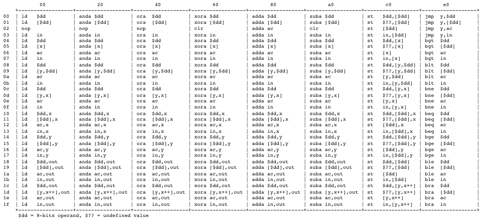
When pondering on the glitch suppression, it occurred to me that the /WE signal also carries some phase information. This can help and prevent us from having to connect a patch wire to the CLK1 breakout. Furthermore, there may be an alternative method to trigger expansion bus operations (other than decoding address lines): using the combined /OE and /WE signals. For regular instructions, at most one of /OE and /WE will be active. After all, you can't read from RAM and write to it at the same time. In the instruction table the opcodes that attempt a read/write combination have their data undefined (operand "$??").

These instructions are valid in the sense that they don't break anything. The data sheet tells what happens to the RAM:

Data sheet 62256 RAM
Screenshot 2019-02-24 at 15.51.35.png (32.84 KiB) Viewed 6369 times

The RAM simply gives precedence to /WE over /OE: it won't try to put data on the bus while also reading from it. This is a protection mechanism of course, but we can use it to our advantage. In a standard Gigatron it just means that it is writing uninitialised data into RAM.

So here's a new idea:

Code: Select all

/IOSEL = /OE | /WE

         _   _   _
CLK     | |_| |_| |_
        ____     ___
/OE         |___|
        ______   ___
/WE           |_|
        ______   ___
/IOSEL        |_|
This can drive the output flip-flops (for example a 74'273). As the data bus itself will be in tristate, the flip-flops should take their data from somewhere else. We'll come back to that in a moment.

First observe that, now that we have data bus in tristate with the RAM reading, we could just as well pass external data lines through a buffer (74'244) to the bus. This gives us 8 lines of input in the same instruction.

Now we have to figure out where the data for the output flip-flops is coming from. I haven't thought that through yet.

One idea is to use address lines again, for example A8:A15. Except that this doesn't quite fly (yet), because those are also addressing the RAM, to which we're now writing. We could add two 74'157s in the same way as in the MAU, and force the RAM to address the zero-page during this cycle. However, that's 2 chips, and they get inserted on the critical path of the Gigatron cycle.

Another idea is to take these bits from the data bus one cycle before, using another 74'273 register. But that chip needs to be clocked by something.

Also, accidental I/O can still happen, especially during boot time(*). If several slave enable lines come from individual flip-flops, we can't just wait until the software initialises them: there is the 350 ms delay by the MCP.

Food for thought....


(*) I see now that this is the point of both the inverters behind the /CSn flip-flops and the hardware triggered reset. That answers my older note 12. So my schematic above is still not right anyway.
Attachments
Expansion2.zip
KiCad files
(13.81 KiB) Downloaded 285 times
Expansion2.pdf
Print version
(148.06 KiB) Downloaded 290 times
monsonite
Posts: 101
Joined: 17 May 2018, 07:17

Re: Expansion bus

Post by monsonite »

Marcel,

Many years ago (1981) I bought an expansion board for a ZX81. For 8-bit output it used a '273 and for 8-bit input a '244.

There was probably another device like a '139 to decode /IORQ and some of the address lines - It was as simple as that.


Ken
User avatar
marcelk
Posts: 488
Joined: 13 May 2018, 08:26

Re: Expansion bus

Post by marcelk »

I just realise my previous rambling doesn't really work for the input scenario: /IOSEL comes too late. It must be derived from /W instead:

Code: Select all

/IOSEL = /OE | /W

         _   _   _
CLK     | |_| |_| |_
        ____     ___
/W          |___|
        ____     ___
/OE         |___|
        ____     ___
/IOSEL      |___|    <-- input through 74'244 to bus(*)
        ______   ___
/WE           |_|    <-- bus to RAM
But /W is on the main board, not on the RAM socket, and without breakout. For a one-off solution you can always solder a patch wire to an IC.

[Edit: (*) this doesn't really work either due to bus contention in φ1 --MvK]
monsonite wrote: 24 Feb 2019, 18:28 It was as simple as that.
I hope it will look simple once it's done. For now it's still a bit like that Apollo 13 situation, where they have to find a way to hook up a square CO2 scrubber to a round air filter, using only parts at hand.


Apollo 13 (1995) - Square Peg in a Round Hole Scene (7/11) | Movieclips
Screenshot 2019-02-24 at 21.29.49.png (455.12 KiB) Viewed 6350 times

Except that we have plenty of time. To be continued next week.
jwolfram
Posts: 18
Joined: 07 Jan 2019, 20:11

Re: Expansion bus

Post by jwolfram »

Marcel, I think Your idea with the $?? operand is excellent. It should make it possible to do I/O without touching RAM and probably to avoid glitches. Here are some new thougths:

- WE_RAM is /WE OR NOT(OE) to prevent write to RAM at this commands
- IOSEL is active if /WE and /OE low and registers the signals (MOSI/CS1,CS2,SCK)
- if SCK is HIGH, both RAMs are disabled (CS=HIGH)
- if SCK is HIGH and /OE is low, MISO will sent to D0 (Tristate buffer)

Code: Select all


    ld      [$countvar]
    bge     no_spi
    ld      $spi_routine_h,y
    jmp	    y,$spi_routine_h

no_spi:
    ;here follows the sound code

spi_routine:

    suba    $0x10                 ;next cycle
    st      [$countvar]           ;store back
    ora     $0xF8,y               ;calc Y with clock LOW
    ld      [$datvar],x           ;get write data
    st      $??,[y,x]             ;this will set MOSI
    xora    $0x04,y               ;calc Y with clock HIGH   
    st      $??,[y,x]             ;this will set SCK and disables RAM
    xora    $0x04,y               ;calc Y with clock LOW   
    ld      [0x00]                ;RAM is disabled and we get MISO at D0
    st      $??,[y,x]             ;this will set SCK to low and re-enables RAM
    anda    $0x01                 ;we need only bit 0
    adda    [$datvar]             ;add data
    adda    [$datvar]             ;add again (shift * 2)
    st      [$datvar]             ;write back

    ;here we can jump to the sound output end...
    
Joerg
User avatar
marcelk
Posts: 488
Joined: 13 May 2018, 08:26

Re: Expansion bus

Post by marcelk »

Indeed, I believe that will work. The SPI mode is restricted, but that's fine. Or we just use more flip-flops and untangle the RAM /CE from SCK.

Software-wise, our video/sound loop has no free cycles during the horizontal pulse (let alone three of them). But we could try to transfer 8 bits in one SYS operation. When running in video mode 1, it will then still be twice as fast (and not pause the sound). And it will be even faster in the higher video modes. Moreover, being synchronous with user code should simplify its application. If done well, it can be faster than Loader, which maxes out at 28k8 payload bits/second.

The 2nd 32K of RAM is now optional.

We can use the second SPI channel to drive an optional MCP23S17 as Ken suggested and get 16 GPIO pins.
User avatar
marcelk
Posts: 488
Joined: 13 May 2018, 08:26

Re: Expansion bus

Post by marcelk »

Blinkenlights on the RAM board have become a must-have in the industry:

Screenshot 2019-02-27 at 20.15.23.png
Screenshot 2019-02-27 at 20.15.23.png (530.69 KiB) Viewed 6275 times

https://youtu.be/V5T3_7feo1U?t=32
User avatar
marcelk
Posts: 488
Joined: 13 May 2018, 08:26

Re: Expansion bus

Post by marcelk »

The glue logic would look like this:

Code: Select all

/O_SEL  =  /OE |  /WE    # Write to I/O
/WE_RAM = ~/OE |  /WE    # Disable RAM write during I/O
/I_SEL  =  /OE | ~SCLK   # Read from I/O
/OE_RAM =  /OE |  SCLK   # Disconnect RAM from bus during I/O
So we need four OR gates and 2 inverters. If we squeeze, this can be done by three chips: 74'175 (Quad Flip-Flop), 74'32 (Quad OR), 74'240 (Octal Inverting Buffer). The last to provide us with 4 buffers and 4 inverters, just to save one chip.

Now we give each SPI device its own MISO line. That eliminates the concern about MISO contention during power-on.

The MISO lines need a pull-up or pull-down resistor to handle the case of unconnected peripherals.

We should still put the 4 buffers on all 8 bus lines. Maybe there is a specific arrangement for the MISO lines that makes the software simpler.

We have 2 inputs left for general purpose input. (But perhaps they should be wired to 0 and 1, and used to encode a board type ID.)

One of them can also be used for physical SD Card detection. (But such a switch can just as well be connected to an independent LED.)

The '175 provides both SCLK and ~SCLK. That is also nice if we want other SPI devices that use a different mode.

~/OE is made by the '240, so we have 3 inverters remaining. Two inverters can correct the MISO data if we feel the software can't do that. The last inverter can be used to invert A15 if we hookup a second 32K RAM.

The RAM expansion is optional now:

2 x 32K:

Code: Select all

/CE_RAM0 =  A15
/CE_RAM1 = ~A15
1 x 32K:

Code: Select all

/CE_RAM0 =  A15
Instead of the standard Gigatron's

Code: Select all

/CE_RAM0 =  L
Because selecting with A15 should be correct as well. If we address the upper memory for reading, the bus is now floating. Only in theory you can craft a program in EEPROM that does that indefinitely. This is not good for the 74HCT inputs of the ALU: they will oscillate. Just don't do that...

From here many variations are possible:
  1. Use an octal flip-flip for 4 more general purpose outputs ('175 --> '273)
  2. Use an octal buffer for 4 more general purpose inputs ('240 --> '244, and add something like a '04 for inverters)
  3. Use a single large RAM (saves a socket, and frees up an inverter in case we need one)
  4. Add the SD Card socket (will need a 3.3V regulator and a logic level shifter. Any through-hole suggestion for that?)
  5. Add the MCP23S17 I/O port expander for 16 GPIO pins (is a maximum of one of those really enough? Otherwise we should go straight for the '273 for at least 4 SPI ports)
If we opt for that last idea ('273 + '240 + '32), we've created 4 SPI ports using 3 chips, and best of all: we're only using part numbers that are already in the Gigatron Bill of Materials to begin with, even the resistor array...
User avatar
marcelk
Posts: 488
Joined: 13 May 2018, 08:26

Re: Expansion bus

Post by marcelk »

Here's a new schematic for the evolving concept.

Inline image
Inline image
Expansion3.png (914.36 KiB) Viewed 6207 times

Ken suggested using a 32-pins RAM socket. With this you can put in the original 32K chip, or upgrade with a single 64K or 128K chip. I added a 74'00. Space-wise this is still a win, and finally there is a true 7400 in the design! That chip can bank any 32K block into the upper half of the RAM address space. (And that addresses my earlier "Note 3" as well...). Wait, I should call it the "MMU"...

Next I replaced the 74'240 with a 74'125 to win back some pins, and to remove the need for letting the software invert incoming data. Not that that is any real issue, and maybe I change it back later. For now we lost the possibility to upgrade to 64K by adding a second 62256 32K (not enough inverters).

Artist impression of the real estate now involved:

Dummy layout
Dummy layout
IMG_4826.jpeg (104.71 KiB) Viewed 6207 times

I didn't draw any MCP23S17 in there yet. There is a 2x3 header block for each of the four SPI ports, so you can always guide a 6-way ribbon cable out of the case, and create your GPIO pins there where you need them. Up to 64 of them!

The MicroSD card socket isn't integrated yet either. I'm not sure anymore if that is really needed? You can get cheap breakout boards from places like SparkFun and AdaFruit with an SMD level shifter already in place. Unfortunately they're mechanically different from each other.

MicroSD breakout board
AdaFruit.jpg (12.49 KiB) Viewed 6207 times
MicroSD breakout board
SparkFun.jpg (20.13 KiB) Viewed 6207 times
Attachments
Expansion3.zip
CAD files
(15.66 KiB) Downloaded 288 times
Expansion3.pdf
Print version
(196.6 KiB) Downloaded 319 times
jwolfram
Posts: 18
Joined: 07 Jan 2019, 20:11

Re: Expansion bus

Post by jwolfram »

I think, the shortcuts between BUS0/BUS4... are not so good.

Joerg
User avatar
marcelk
Posts: 488
Joined: 13 May 2018, 08:26

Re: Expansion bus

Post by marcelk »

Those pesky electrons...
Post Reply