Expansion bus

Using, learning, programming and modding the Gigatron and anything related.
Forum rules
Be nice. No drama.
User avatar
marcelk
Posts: 488
Joined: 13 May 2018, 08:26

Re: Expansion bus

Post by marcelk »

I updated the schematic. For now I will just leave the 4 upper bus lines floating. There're tons of things to (re)consider, but this revision looks good enough for a first spin and to get something to toy around with.

Inline image
Inline image
Expander-schematic.png (1008.69 KiB) Viewed 8242 times

I don't feel like building this on a breadboard. A quick layout for the prototype looks like this. It will obstruct the RAM, MAU and X/Y register area. The top-right should just miss the MCP450.

3D model
3D model
7358201551541622976.jpg (91.85 KiB) Viewed 8242 times

As a sanity check of the ideas, I also forced myself to write down the youngest concept on hackaday.io:
https://hackaday.io/project/164176-giga ... m-expander
Attachments
Expander-schematic.pdf
Circuit diagram
(186.85 KiB) Downloaded 372 times
jwolfram
Posts: 18
Joined: 07 Jan 2019, 20:11

Re: Expansion bus

Post by jwolfram »

Yesterday I started with a concept to add this to my emulator. An I found two topics which are IMHO worth for discussion.
At first, the MOSI line. I think its better to get it from A15 instead of A7. If You use A7, the data to output must be build from bit 7 of the data to shift and the control lines. But I found a probably better solution:

Code: Select all

A0  ->  SCLK
A1  ->  (unused)
A2  ->  CS0
A3  ->  CS1
A4  ->  CS2
A5  ->  CS3
A6  ->  BankSel 0
A7  ->  BankSel 1
A15 ->  MOSI
D0 and D1 remains always zero in the ctrl register. By using x++ we can toggle the SCLK line without additional instructions:

Code: Select all

    ld   [cltr_reg],x      ;get ctrl byte from zeropage
    ld   [data_reg],y      ;get data byte from zeropage
    st   $??,[y,x++]       ;set ctrl lines, SCLK is low
    st   $??,[y,x++]       ;set SCLK high
    ld   [0x00]            ;read I/O data
    anda 0x01              ;we need only this bit
    st   $??,[y,x++]       ;set SCLK back to LOW because we need access to the RAM
    adda [data_reg]        ;add the original data..
    adda [data_reg]        ;..shifted left
    st   [data_reg]        ;store back data byte

With those 10 instructions a single bit can be exchanged, 80 are needed for transfer one byte, this will fit nearly twice into one (non-)video line. But for init of the SC-card there must be a slower routine.

The next topic are the four MISO lines. I think, three of them are not necessary and can be used, for instance, for board coding. The problem I see, incoming data mus be shifted into D0 of the data register. Left shifting can be done by adda, but right shifting data can only be done by lookup tables in RAM or anda+beq. So the firmware will need different routines for different SPI ports. SPI slaves have to tri-state their SO line if not selected so the four SPI MISO lines can be connected to the line which drives D0.

Joerg
User avatar
marcelk
Posts: 488
Joined: 13 May 2018, 08:26

Re: Expansion bus

Post by marcelk »

Excellent!

The ROM builder emits some information about available cycles on different scan line types.

Code: Select all

runVcpu at 014a cycles 100 info line0
runVcpu at 019a cycles 130 info line1-39 typeC
runVcpu at 01a1 cycles 134 info line1-39 typeABD
runVcpu at 01db cycles 126 info line40
runVcpu at 02ec cycles 148 info line41-520 typeBCD
This means the SYS instruction must fit in 148 cycles. Or ≤134 cycles if we want to maintain some minimum I/O level when the system is in video mode 0. From this, the vCPU+SYS overhead of 20 cycles still must be subtracted. That makes handling of 16 bits per scan line a rather high goal. If we achieve 8 bits we can hope to make the SYS function self-restarting and eliminate the loop overhead for multibyte transfer. (Much like the sprite functions that are self-restarting as well.)

Indeed, the masking and branching sets us back 3 cycles. We use the branch delay slot to keep it small. I think we can win one cycle back in the last instruction, for a total of 12 cycles per bit transfer. Like this:

Code: Select all

        ld      [data_reg],y ;once
        ld      [ctrl_reg],x
        st      $??,[y,x++]
        st      $??,[y,x++]
        ld      [$00]
        st      $??,[y,x]
        anda    [miso_mask]
        beq     .label
        bra     .label
        ld      $01
.label: adda    [data_reg]
        adda    [data_reg]
        st      [data_reg],y
We'll have an unrolled loop anyway, and could address each bit directly if we so desire. This is a nice moment to reflect that 12 cycles take less than 2 microseconds...

I coin the mnemonic 'ctrl' for our new instruction. Maybe it should have its operands given without brackets, because we're not addressing RAM. Like so:

Code: Select all

        ctrl    y,x++
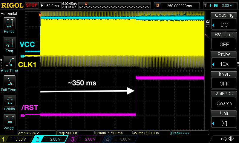
The point for the split MISO lines is primarily around the power-on behaviour. The /SS lines come up in an arbitrary state that lasts for 350 milliseconds before software starts running:

Power on sequence
Power on sequence
photo_2019-02-23_21-12-57.jpg (72.05 KiB) Viewed 8225 times

[Well, technically, software is running in that time, but only repeating the instruction at ROM address 0.]

The point is, if multiple peripherals can drive a shared MISO line in this phase, that creates a short circuit.

We don't have a reset line on the RAM socket that can reset the flip-flops from hardware land. Adding another MCP450 power-on reset component alone doesn't solve it, because we've lost the output inverters along the way. It would also be nice if the user can't create a short circuit from software land.


Edit 1: Changed last "st $??,[y,x++]" to "st $??,[y,x]" because the increment is not used.
Edit 2: Moved "st $??,[y,x]" before "anda [miso_mask]" because RAM is still disabled otherwise.
Note: Alternatively, "anda [miso_mask]" can become "anda 0xf" if the MISO lines are pulled-down.
Edit 3: Fixed conditional sequence
jbailey
Posts: 28
Joined: 20 Nov 2018, 08:54

Re: Expansion bus

Post by jbailey »

With all of the work on getting an SPI interface implemented, have you considered the ability to tie two Gigatrons together over an SPI port. Then have one dedicated to Video, Audio, and the other acting and the CPU and serial IO?

This would be a very cool way to get a really fast computer from a set of them... just a thought.
Last edited by jbailey on 08 Mar 2019, 02:55, edited 2 times in total.
User avatar
marcelk
Posts: 488
Joined: 13 May 2018, 08:26

Re: Expansion bus

Post by marcelk »

All of the above is about implementing master mode. Slave mode is a different story. You run into the some different considerations when you don't control the clock, much like with PS/2. However for a duo configuration you don't need an expander. You can have one system's OUT port (U37) hooked the other's input (U39) directly. You can even replace the 74HC595 shift register with an 74'244 octal buffer for an 8 bit parallel bitstream from one to the other. That chip is on the original breadboard design BTW.

I've pushed some untested code in GitHub. Byte transfer is now an auto-repeating SYS extension of 130 cycles, good for exchanging anywhere from 1 to 256 bytes in one go. This can be a start for experimentation.
jwolfram
Posts: 18
Joined: 07 Jan 2019, 20:11

Re: Expansion bus

Post by jwolfram »

Transfer a fixed number of bytes is suitable for writing to a SD card but not for reading. For init (must be do at low frequency) and read we need polling. I will explain how I did SD-card access in my library:

Read sector:
  • set CS to LOW
  • send 2 times 0xFF (dummy, for sync)
  • send 0x17, address and checksum (can be dummy)
  • send 0xFF until 0xFE (start block token) is received
  • send 512 times 0xFF and receive sector data
  • send 2 times 0xFF and ignore data (checksum)
  • set CS to HIGH
Write sector:
  • set CS to LOW
  • send 2 times 0xFF (dummy, for sync)
  • send 0x24, address and checksum (can be dummy)
  • send 0xFE (start block token)
  • send 512 bytes sector data
  • send 2 times 0xFF (dummy checksum)
  • set CS to HIGH
Joerg
Attachments
sdcard.c
(9.71 KiB) Downloaded 385 times
User avatar
marcelk
Posts: 488
Joined: 13 May 2018, 08:26

Re: Expansion bus

Post by marcelk »

Thanks! It looks doable with the current SYS functions already. We can make some dedicated ones as well. Now I'm debugging the protoboard. It got in yesterday morning. I still had to fix a cycle count error in my bit transfer code snippet (I edited the post above accordingly). I decided on using the WozMon for testing the board. No PC or laptop needed :-). With a LED I could easily determine that I can drive the enable lines of each SPI port. The next step is to send data. Here is what it looks like:

Testing SPI transfer
IMG_4838.jpeg (282.7 KiB) Viewed 8117 times
The code does this:

Code: Select all

11 00 05  LDWI 0500 ;Send page (begin address)
2B 24     STW  24
11 03 06  LDWI 0603 ;Receive page (end address)
2B 26     STW  26
11 09 0B  LDWI 0B09 ;SYS_Control_v3x_40
2B 22     STW  22
59 78     LDI  78   ;Enable SPI0
B4 FA     SYS  FA   ;(270-40/2)
11 00 0D  LDWI 0D00 ;SYS_SpiTransfer_v3x_130
2B 22     STW  22
B4 CD     SYS  CD   ;(270-130/2)
11 09 0B  LDWI 0B09 ;SYS_Control_v3x_40
2B 22     STW  22
59 7C     LDI  7C   ;Disable all
B4 FA     SYS  FA
FF        RET       ;Return
Result on the scope:

First SPI signals
First SPI signals
IMG_4840.jpeg (172.28 KiB) Viewed 8117 times

It looks promising on the scope. We are sending out the expected data while the Gigatron maintains its video signal. The longer gap after the first byte is caused by a VGA pixel burst, during which the application is stalled. This is all good.

However, the input still comes in as all-ones where I expect all-zeroes. The input lines look noisy as well. As if the pull-down resistors don't do anything. This needs some investigation. I'm using 22K resistors for now and that could be too high allowing the traces to pick up crosstalk. [Edit: bending the resistors had broken off some of them. That explains the noisy MISO signal and the all-ones input. The resistor values should be lowered as well.]

Here's the patched board in my test setup:

Patched prototype board
IMG_4839.jpeg (200.96 KiB) Viewed 8117 times
User avatar
marcelk
Posts: 488
Joined: 13 May 2018, 08:26

Re: Expansion bus

Post by marcelk »

I got to control the MCP23S17, movie here: https://www.youtube.com/watch?v=3ugpzAZGCHQ

This is a rather complex chip: it has 22 internal registers for controlling its behaviour and it can generate interrupts. I like that it is outside the case, just like Pluggy. No complex chips are allowed inside! (Although we're gradually losing the "single-board" claim.)

Test setup
Test setup
IMG_4846.jpeg (359.72 KiB) Viewed 8076 times
In this demo we're using two commands:

Code: Select all

40 00 00 ; Set PORTA to all-output

40 14 xx ; Send byte value xx to PORTA
I verified the SPI reading as well (0x41 command byte), and it works as expected.

The code in the video reads as below. It simply sends the frame counter out until a key is pressed. This counter increments 60 times per second.

Code: Select all

0050 59 40    LDI  $40   ; MCP23S17 Write
0052 5E 78    ST   $78
0054 59 78    LDI  $78   ; Send buffer (start address)
0056 2B 24    STW  $24
0058 E3  3    ADDI 3     ; Receive buffer (end address)
005A 2B 26    STW  $26
005C 11  9  B LDWI $B09  ; SYS_Control
005F 2B 22    STW  $22
0061 59 78    LDI  $78   ; Enable SPI0
0063 B4 FA    SYS  $FA
0065 11  0  D LDWI $D00  ; SYS_SpiTransfer
0068 2B 22    STW  $22
006A B4 CD    SYS  $CD
006C 11  9  B LDWI $B09  ; SYS_Control
006F 2B 22    STW  $22
0071 59 7C    LDI  $7C   ; Disable SPI0
0073 B4 FA    SYS  $FA
0075 FF       RET
0076 50  0    .WORD $0050

00A0 75       PUSH
00A1 59  0    LDI  0     ; MCP23S17 IODIRA register
00A3 2B 79    STW  $79
00A5 CF 76    CALL $76   ; IODIRA = 0 (output)
00A7 59 14    LDI  $14   ; MCP23S17 OLATA register
00A9 5E 79    ST   $79
00AB 1A  E    LD   $0E   ; Gigatron frameCount
00AD 5E 7A    ST   $7A
00AF CF 76    CALL $76   ; OLATA = [frameCount]
00B1 1A  F    LD   $0F   ; Gigatron serialRaw
00B3 8C FF    XORI $FF
00B5 35 3F A5 BEQ  $00A7 ; Continue until key pressed
00B8 63       POP
00B9 FF       RET
These chips can be chained, with up to 8 of them sharing the same SPI controls. So this gives a potential of 4x8x16 = 512 GPIO pins.
mwwhited
Posts: 1
Joined: 17 Mar 2019, 06:36

Re: Expansion bus

Post by mwwhited »

Based on the opcode/expansion bus work so far... would it be possible to just add a new register (say MMU / DMA) that would use the ST /OE & /WE [$dd] Adding banked memory would open many options including dedicated video buffer pages. If we can move the video to an external controller circuit/memory most of the CPU time can go back to code. If my math is correct it should also allow for up to 16MB of paged memory.

Doing this some pages could be reserved for IO such a using a dedicated page as a ring buffers for SPI/UART. The dedicated addresses would allow for slave SPI at speeds isolated from system clock. It could even open up adding dedicated audio, UART, lpt. Who knows... more system process clock and maybe even USB or Ethernet.
User avatar
marcelk
Posts: 488
Joined: 13 May 2018, 08:26

Re: Expansion bus

Post by marcelk »

The 4-chip concept (7400+7432+74125+74273) has a 2-bits "MMU", thereby supporting every byte of the commonly found 32-pins 128K memories. But you can play with the number of MMU bits vs. the number of SPI ports if you find a way to get more logic gates in there to expand the bank selector. Now it uses 2 NAND gates of the 7400 for that, and the other two are used as inverters for the control logic. The 3-chip proposal that it was derived from (7432+74240+74273) could only support SPI and up to 64K of memory because it is lacking the logic gates for the selector. So the current prototype already deviates from the minimalism that defines the Gigatron. Ouch. Perhaps we should return to 3 chips for that reason. Anything is possible when you allow for too many chips...
Post Reply